NEWS
12
Aug

Porous Ceramic Vacuum Chucks: The Essential Guide for Semiconductor and Precision Manufacturing

Share:

Introduction


In semiconductor fabrication and advanced electronics manufacturing, holding thin, fragile workpieces — silicon wafers, glass substrates, ceramic plates — without inducing stress, deformation, or surface damage is one of the most critical challenges in the process chain. Traditional mechanical clamping introduces point loads that crack brittle materials, while standard metal vacuum chucks with drilled holes create localized pressure differentials that deform ultra-thin substrates. The solution that has become indispensable across the industry is the porous ceramic vacuum chuck.

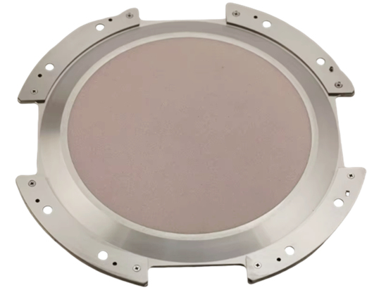
                                    Ceramic Vacuum Chucks


This comprehensive guide covers the working principles, manufacturing processes, selection criteria, and application landscape of porous ceramic vacuum chucks, with insights from More Superhard's expertise in advanced ceramic materials and precision grinding technologies.

1. How Porous Ceramic Vacuum Chucks Work


A porous ceramic vacuum chuck exploits the natural micro-porosity of engineered ceramic materials to create a uniform, full-surface vacuum hold. Unlike conventional metal chucks that rely on a pattern of drilled holes or grooves connected to a vacuum manifold, a ceramic chuck distributes vacuum through millions of microscopic pores that permeate the entire ceramic body.

1.1 Micro-Pore Infiltration


The ceramic material contains a dense network of interconnected micro-pores, typically ranging from 1 to 30 micrometers in diameter. These pores are created during the manufacturing process through the controlled addition and subsequent burnout of pore-forming agents. The resulting pore structure forms a continuous pathway from the vacuum plenum beneath the chuck to the workpiece-contact surface above.

1.2 Uniform Negative Pressure Distribution


When a vacuum is applied to the plenum, negative pressure is distributed evenly across the entire contact surface through the micro-pore network. This means every square millimeter of the workpiece experiences nearly identical holding force — eliminating the localized high-pressure zones that cause thin wafers to bow, warp, or develop stress-induced defects. The result is a flat, stable, and stress-free workpiece hold that is essential for sub-micron precision processes.

2. Core Advantages of Ceramic Vacuum Chucks


2.1 Exceptional Flatness and Parallelism


Ceramic materials such as alumina (Al2O3) and silicon carbide (SiC) are inherently rigid and resistant to deformation under mechanical or thermal loads. After precision grinding and polishing, the working surface of a ceramic chuck can achieve flatness values of 2 micrometers or better across the entire face — a level that is virtually impossible to maintain with polymer or composite alternatives.

2.2 Uniform Hold Without Local Deformation


Because the vacuum is distributed through millions of micro-pores rather than a handful of large holes, the holding force is truly uniform. This eliminates the dimpling, bowing, or local deformation that plagues conventional vacuum chucks when processing wafers thinner than 100 micrometers.

2.3 Wear Resistance and Long Service Life


Engineering ceramics rank among the hardest industrial materials, with Vickers hardness values of 15 to 28 GPa depending on the composition. This extreme hardness translates to outstanding wear resistance: the chuck surface maintains its flatness and pore structure through millions of load/unload cycles, far outlasting metal or polymer alternatives that require periodic re-machining or replacement.

2.4 Chemical and Thermal Stability


Ceramic chucks withstand aggressive process environments including corrosive chemicals used in CMP slurries, high-temperature plasma in etching and CVD chambers, and the extreme thermal cycling of rapid thermal processing. This chemical inertness and thermal stability make them suitable for virtually every step of the semiconductor fabrication flow.

3. Manufacturing Process: From Powder to Precision Component


Producing a porous ceramic vacuum chuck is a sophisticated multi-step process that demands tight control at every stage. The key manufacturing steps are:

3.1 Powder Preparation and Mixing


High-purity ceramic powder — either alumina (Al2O3) or silicon carbide (SiC) — is blended with carefully selected pore-forming agents and organic binders. The type, quantity, and particle size of the pore-forming agent directly determine the final pore diameter (typically 1 to 10 micrometers) and porosity (typically 30% to 40% by volume). This formulation step is where the fundamental performance characteristics of the chuck are established.

3.2 Forming and Green Machining


The powder mixture is shaped into the chuck's preliminary geometry using cold isostatic pressing (CIP) or injection molding. The resulting 'green body' is then machined to near-net shape using conventional tooling, taking advantage of the relatively soft, unfired state of the ceramic compact.

3.3 High-Temperature Sintering


The green body is fired in a high-temperature furnace at 1,500 to 1,800 degrees Celsius. During sintering, the pore-forming agents burn out completely, leaving behind the designed network of interconnected micro-pores. The ceramic particles simultaneously densify and bond together, developing the final mechanical strength and hardness. Precise control of the sintering temperature profile is critical to achieving the target porosity without compromising structural integrity.

3.4 Precision Machining and Polishing


After sintering, the ceramic is extremely hard and can only be machined with diamond tooling. Precision grinding and lapping operations bring the working surface to its final flatness specification — often 2 micrometers or less across a 300 mm diameter. This is where More Superhard's core expertise in diamond and CBN grinding technology directly contributes to achieving the exceptional surface quality that semiconductor-grade ceramic chucks demand.

3.5 Vacuum System Integration


The finished porous ceramic face is bonded to a dense ceramic or metal base (typically stainless steel or aluminum alloy) using high-temperature brazing or specialized adhesive bonding. This assembly creates a sealed vacuum plenum that connects to the facility's vacuum supply. For multi-zone chucks, internal baffles and separate vacuum ports are incorporated to enable independent control of different radial zones.

3.6 Final Inspection and Qualification


Every chuck undergoes rigorous quality verification including laser interferometry for flatness measurement, coordinate measuring machine (CMM) inspection for dimensional accuracy, and vacuum performance testing for pump-down speed and ultimate negative pressure. Only chucks that pass all tests are released for shipment.

4. Selection Criteria: Matching Chuck to Application


4.1 Material: Alumina vs. Silicon Carbide

Alumina (Al2O3) chucks offer an excellent balance of cost, electrical insulation, and mechanical performance for the majority of wafer processing and inspection applications. Anti-static alumina variants are widely available and suitable for most cleanroom environments.
Silicon carbide (SiC) chucks deliver substantially higher thermal conductivity — several times that of alumina — along with lower thermal expansion and greater stiffness. SiC is the mandatory choice for applications involving high thermal loads, rapid temperature cycling, or extreme dynamic acceleration, such as lithography wafer stages and high-temperature etch processes.

4.2 Flatness and Parallelism


Flatness is the single most critical specification for a vacuum chuck in semiconductor applications. General inspection-grade chucks typically require flatness of 5 micrometers or less. For thinning, lithography, and other ultra-precision processes, flatness requirements tighten to 2 micrometers or even 1 micrometer. Any deviation from specification causes wafer warpage that translates directly into yield loss.

4.3 Pore Size and Porosity


Fine-pore chucks with 1 to 3 micrometer pore diameter provide the most uniform vacuum distribution and minimize the risk of backside marking on ultra-thin wafers (below 100 micrometers). Larger-pore chucks with 10 to 30 micrometer pores offer faster pump-down speeds and greater tolerance to particulate contamination, making them suitable for thicker or rougher substrates.

4.4 Electrical Resistivity and ESD Protection


Electrostatic discharge (ESD) can destroy integrated circuits on a wafer. To prevent this, semiconductor-grade ceramic chucks are manufactured with controlled electrical resistivity, typically in the range of 10^6 to 10^9 ohms per square. This dissipative range allows static charges to bleed off safely without creating the sudden discharge events that damage sensitive circuitry.

4.5 Multi-Zone Vacuum Control


Fabrication facilities that process multiple wafer sizes on the same equipment benefit from chucks with independently controllable vacuum zones. By selectively activating or deactivating outer zones, a single chuck can securely hold both 200 mm and 300 mm wafers without vacuum leakage at the uncovered periphery.

5. Key Applications Across the Semiconductor Value Chain


5.1 Front-End Fabrication (Fab)

  • Lithography: SiC ceramic chucks serve as the core component of the wafer stage in advanced lithography scanners, carrying wafers through high-speed positioning and exposure with zero thermal deformation.
  • Chemical Mechanical Polishing (CMP): Ceramic chucks hold wafers during polishing with abrasive slurry, leveraging the ceramic's resistance to chemical corrosion from the slurry's acidic or alkaline components.
  • Etching and Thin Film Deposition (CVD/PVD): Ceramic chucks withstand the high temperatures and energetic ion bombardment of plasma-based processes while providing stable, contamination-free wafer support.

5.2 Back-End Packaging and Testing

  • Wafer Thinning and Dicing: As chips become thinner for 3D stacking architectures, wafers are ground down to tens of micrometers. Porous ceramic chucks provide full-surface support that prevents the thin, fragile wafer from cracking under grinding and dicing forces.
  • Wafer Probing and CP Testing: During electrical testing, probe needles exert significant vertical force on the wafer's bond pads. The extreme hardness and flatness of ceramic chucks ensure reliable probe contact while ESD-safe ceramic protects the circuits under test.

5.3 Beyond Semiconductors: Display, Solar, and Micro-LED

  • OLED and LCD Panel Manufacturing: As display glass substrates grow larger and thinner (0.1 to 0.5 mm), porous ceramic chucks enable damage-free handling during laser lift-off, automated optical inspection, and robotic transport.
  • Micro-LED Mass Transfer: The emerging process of transferring millions of microscopic LED chips from growth wafers to display backplanes relies on vacuum pick-and-place heads built on porous ceramic substrates for precise, simultaneous pickup and release.

Conclusion


Porous ceramic vacuum chucks have become indispensable components in semiconductor fabrication and advanced electronics manufacturing. Their unique combination of uniform vacuum distribution, exceptional flatness, chemical resistance, and long service life addresses the most demanding requirements of modern wafer processing — from lithography and CMP to thinning, testing, and next-generation display assembly.
More Superhard brings deep expertise in advanced ceramic materials and precision grinding technology to every ceramic chuck project. Our team supports customers from material selection and design through manufacturing, qualification, and ongoing process optimization. Contact us at www.moresuperhard.com to discuss how porous ceramic vacuum chucks can improve yield and throughput in your manufacturing line.
 
 
FOLLOW US
This Blog keeps our valued customers informed of important Radiac News and Events, and in the industries we serve.
Copyright © 2003-2023 More SuperHard Products Co., Ltd
Home
Whatsapp
E-mail
Inquiry